METREX™
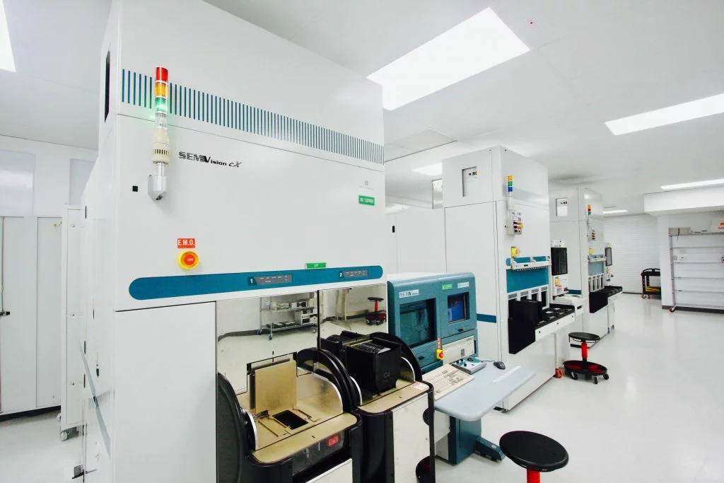
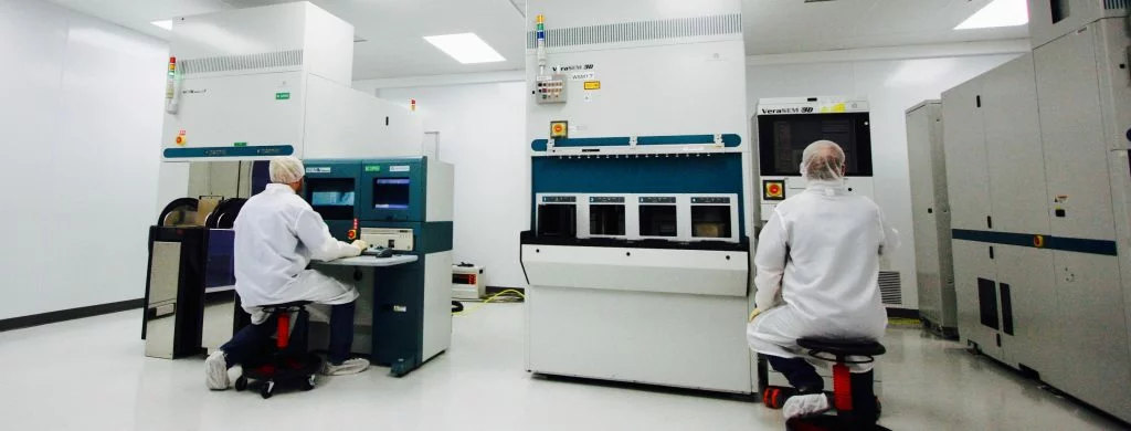
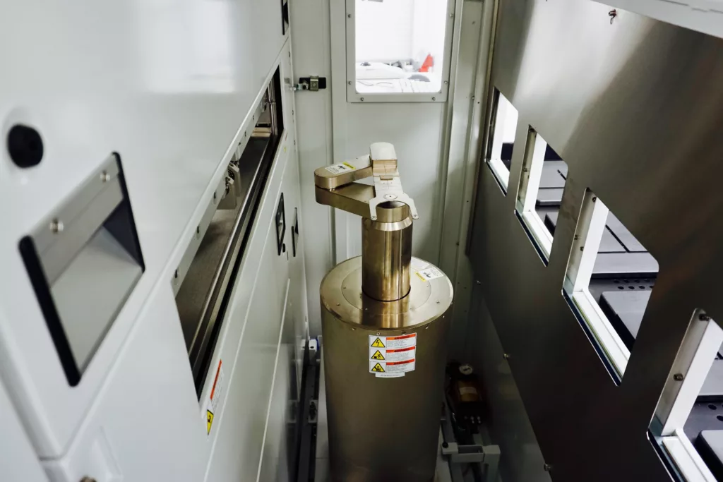
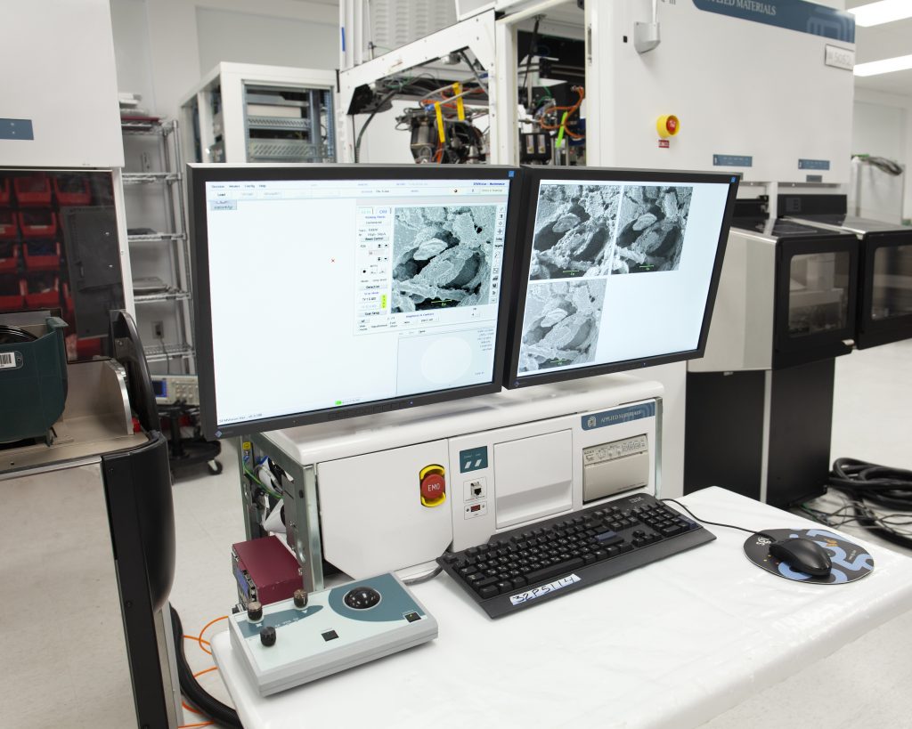
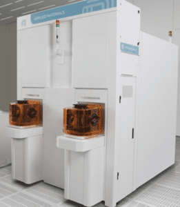
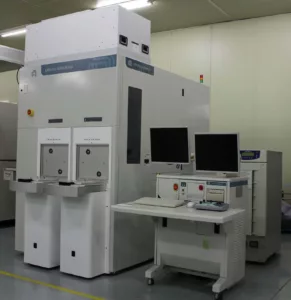
GTI - now known as METREX™ - has been providing metrology solutions for Applied Materials® platforms since 2012. We remanufacture AMAT CD-SEM and DR-SEM metrology systems, offering high-quality equipment at a significant cost and lead time savings over that of new systems. We support our customers with our extensive inventory of +70,000 ready-to-ship spare parts, expert service support, in-house training programs, and foundry capabilities.
RT Experts™
RT Experts™ (RT-EX) specializes in remanufacturing semiconductor MASK systems, enabling customers to access advanced technology at a more affordable price point.
Our Locations
GTi is well-positioned to serve the needs of customers worldwide, with offices in North America, Europe, and Asia. Our goal is to make cutting-edge technology more accessible to businesses of all sizes and locations. With the launch of METREX and RT Experts (RT-EX), we're one step close to achieving that goal.
etrology®
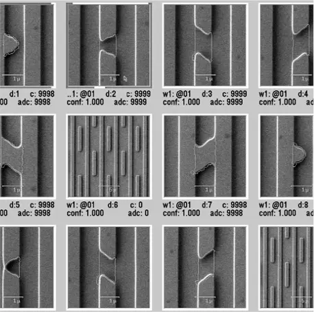
GTI is the exclusive reseller for Etrology Software Innovations
etrology® - the revolutionary solution that offers you unparalleled freedom in measurement and inspection tasks!
etrology® provides innovative solutions in Test & Measurement, Process & Machine, Data Logging, and Automation
etrology® - the revolutionary solution that offers you unparalleled freedom in measurement and inspection tasks!
etrology® provides innovative solutions in Test & Measurement, Process & Machine, Data Logging, and Automation