0
nm
Resolution
0
°
Tilt Function
0
X
Magnification
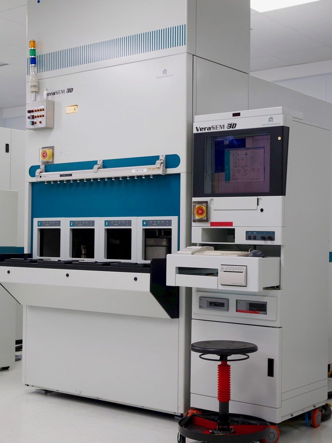
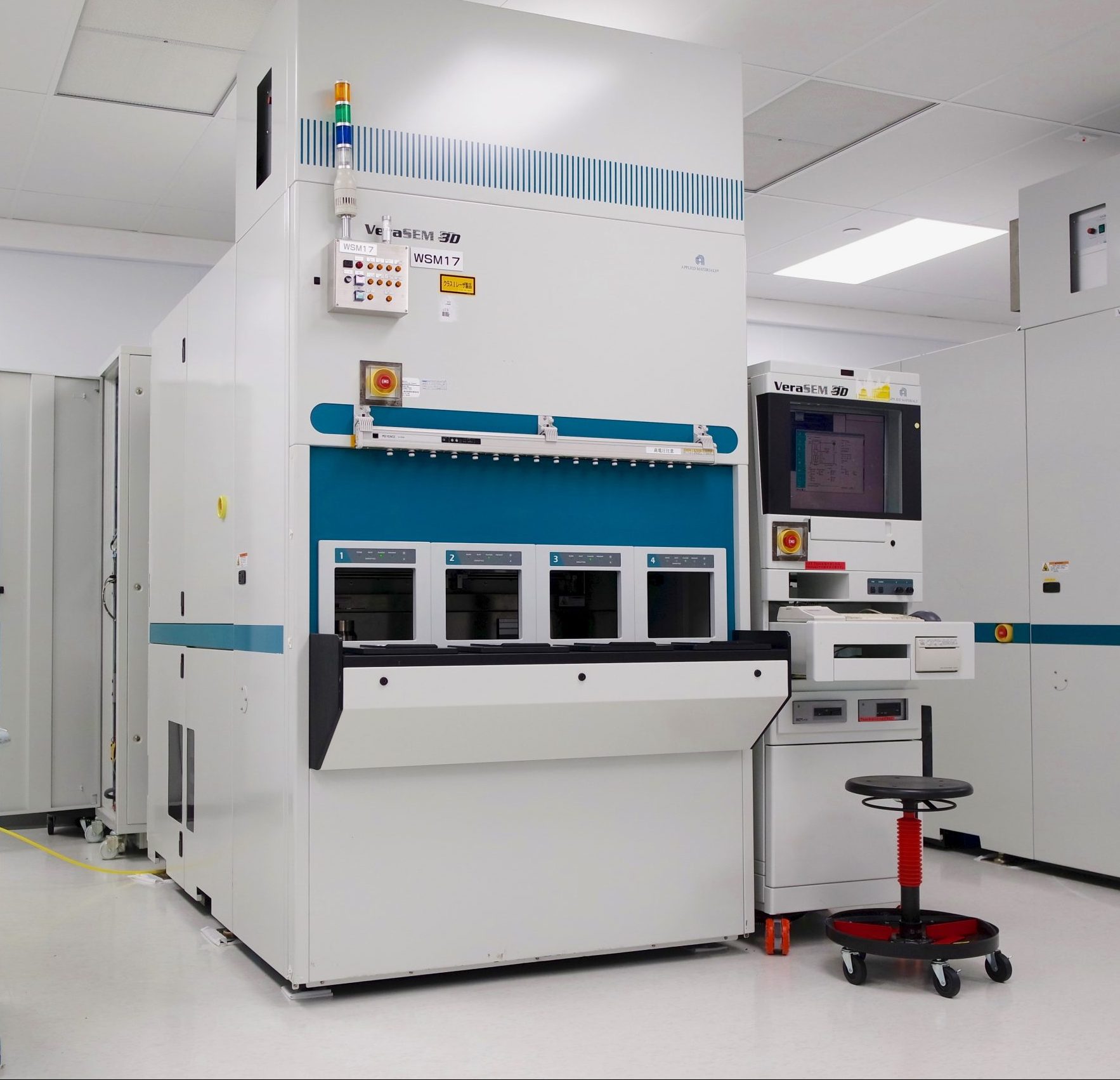
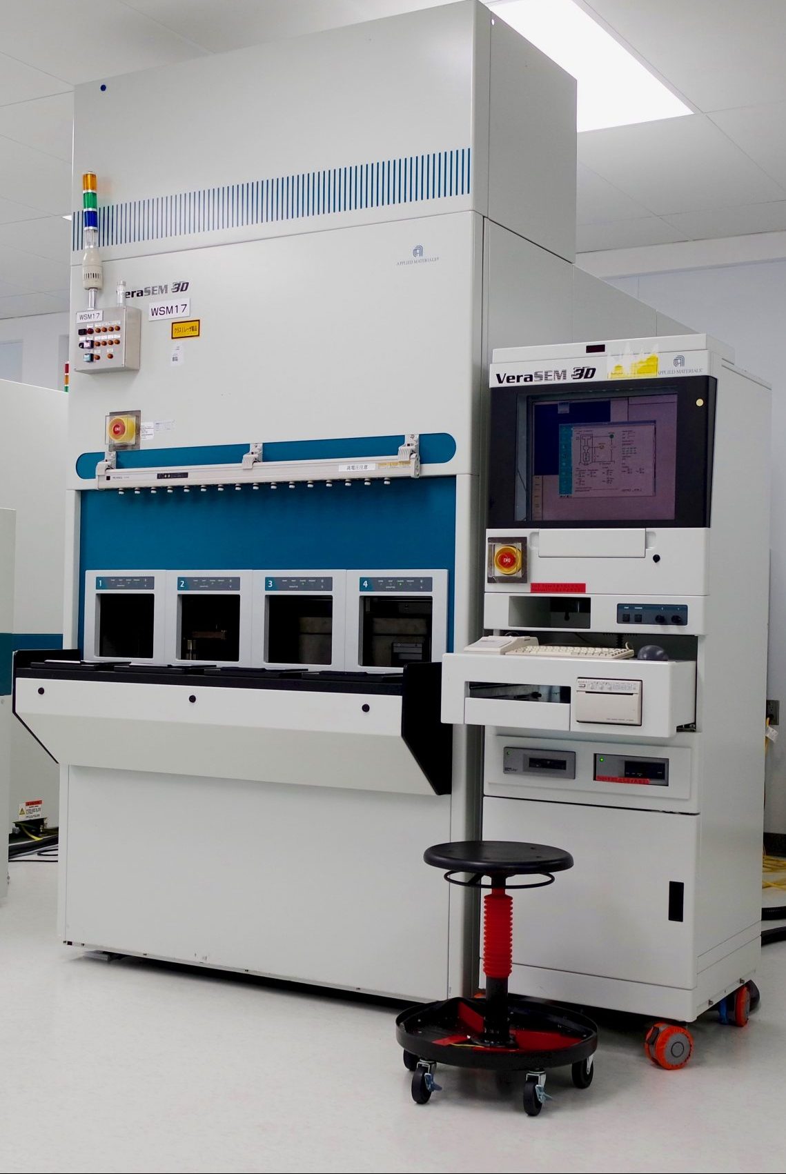
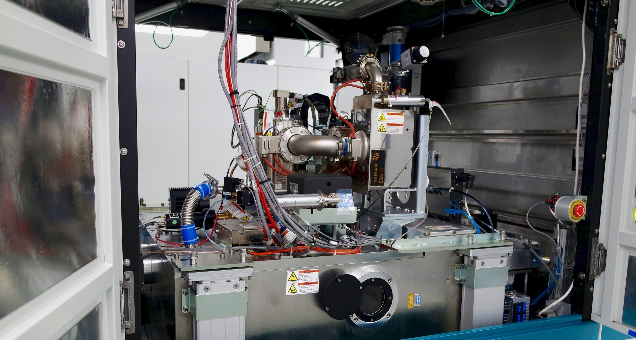
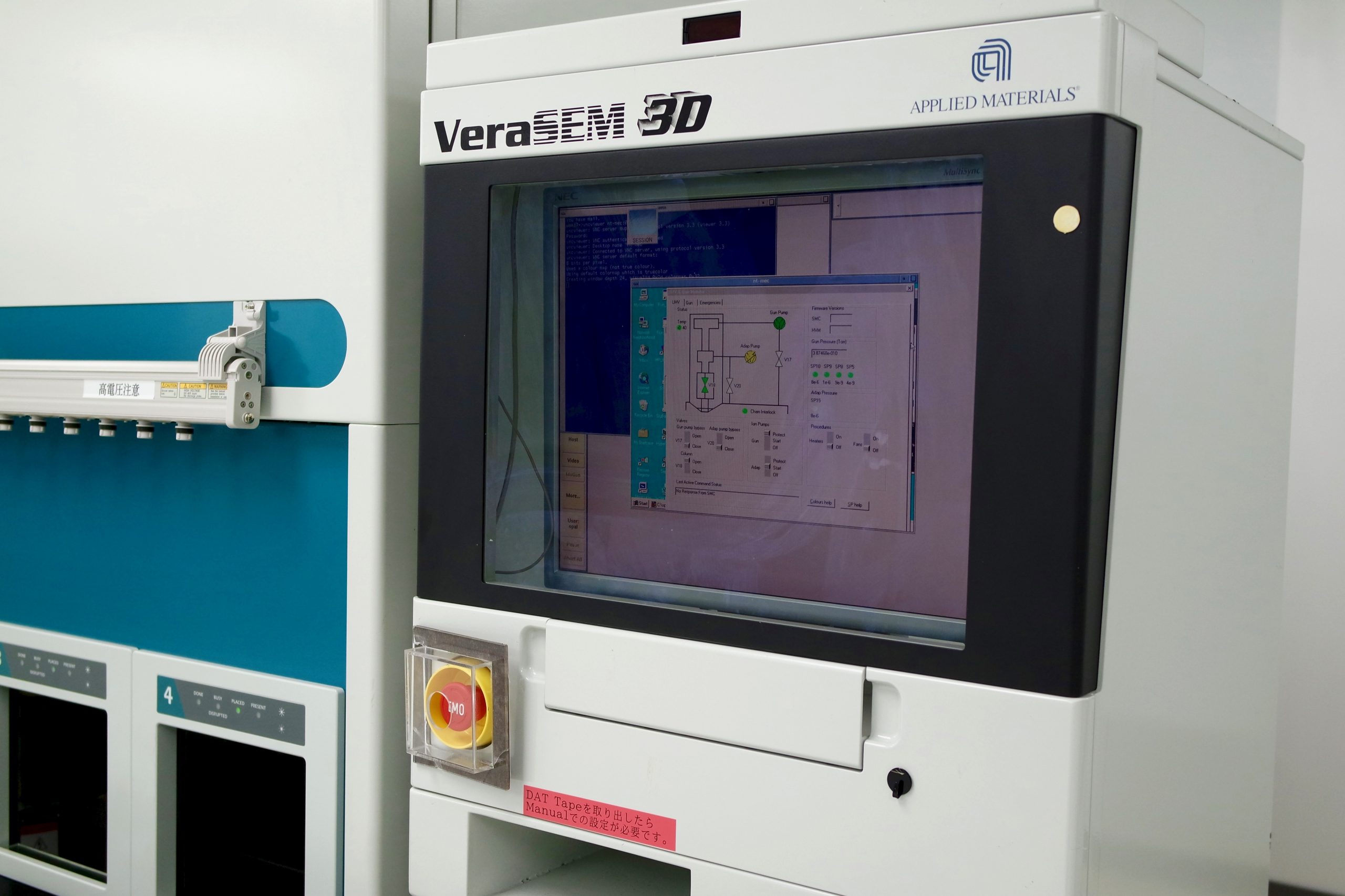
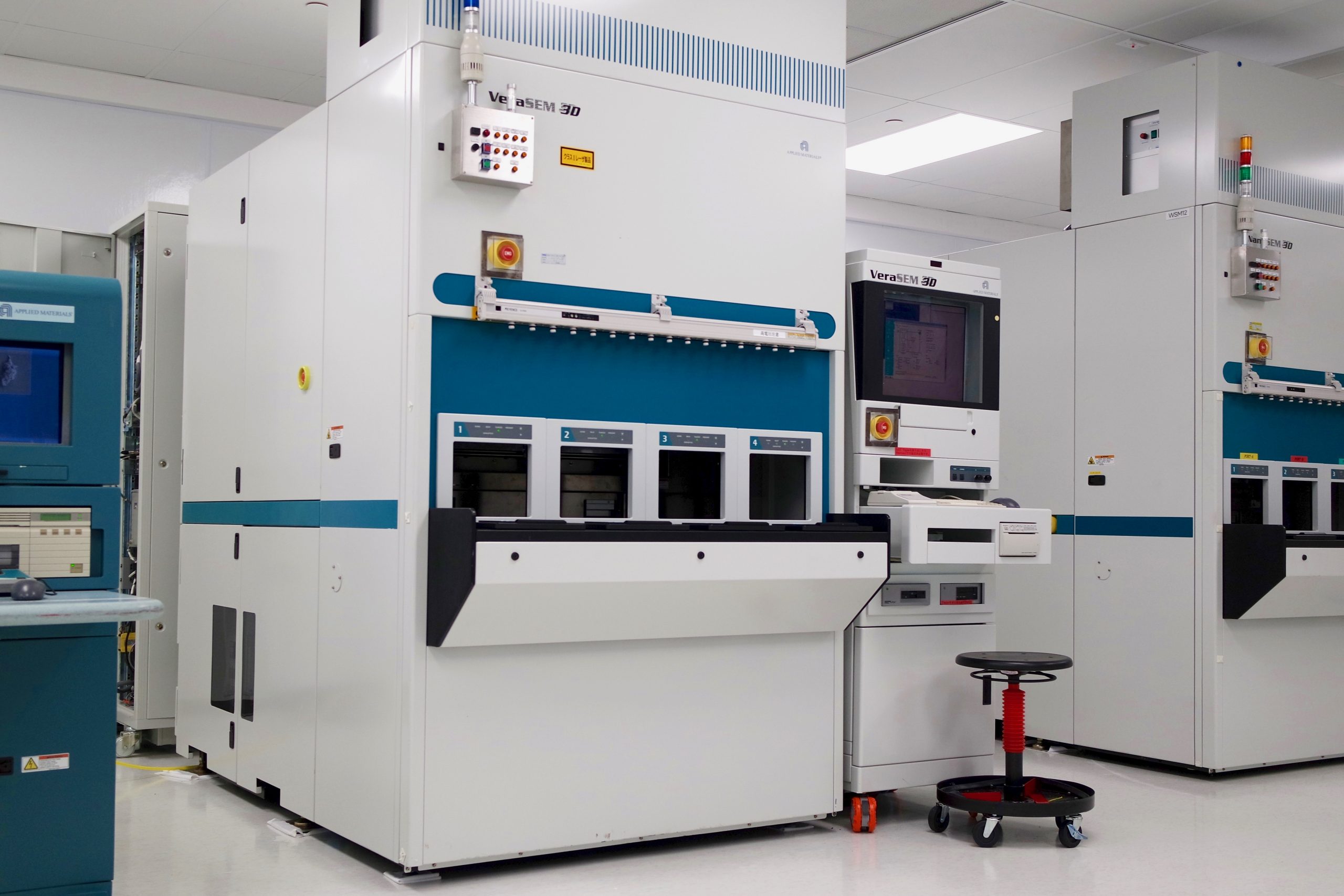
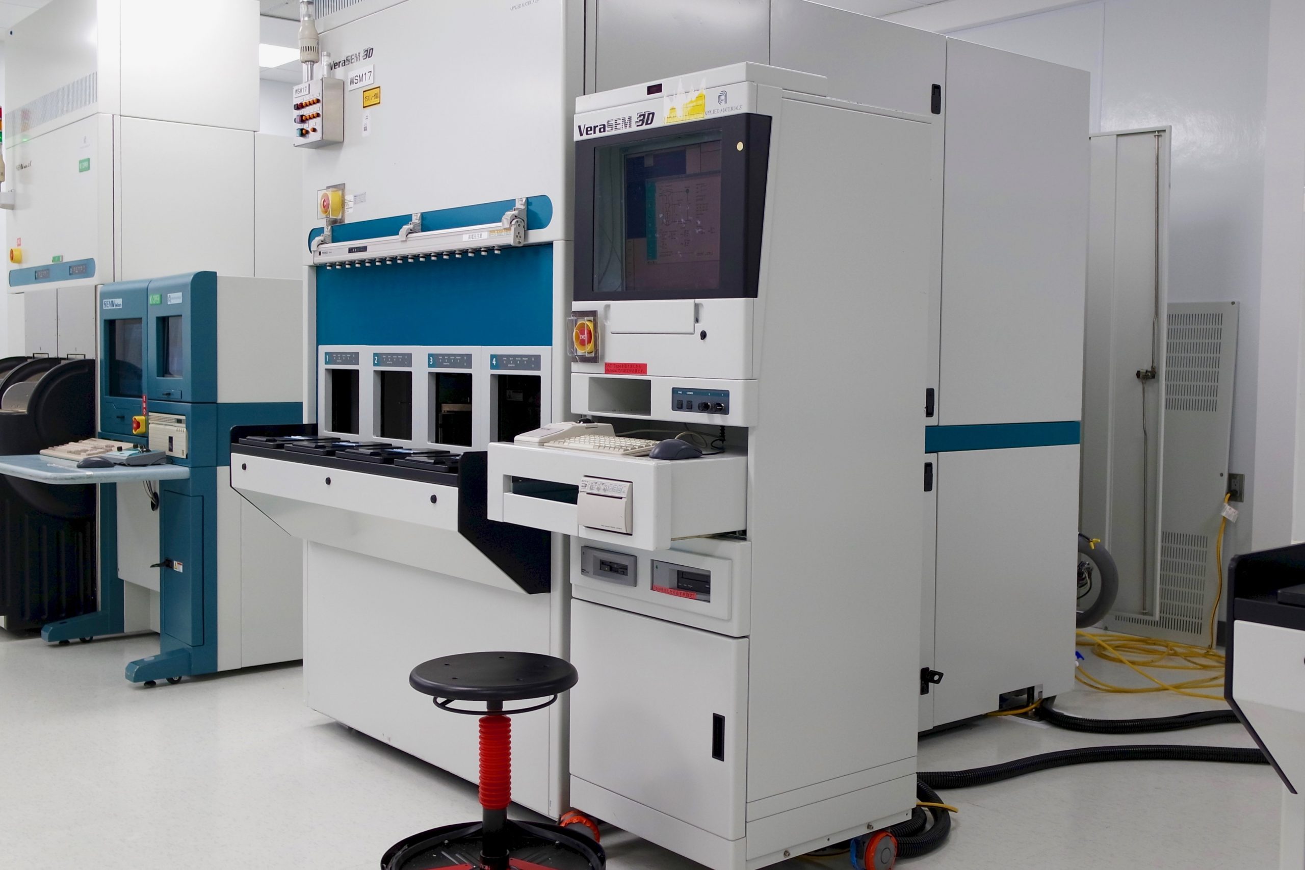
The VeraSEM 3D system’s exceptional in-line accuracy and process control eliminate more time-consuming and costly off-line wafer cross-sectioning while helping chipmakers to streamline process development, improve device performance and yield, and shorten ramp times to high-volume production.
Wafer Specification
- Wafer Size: 200MM
- Wafer Shape: SNNF (Semi Notch No Flat)
- Wafer : 6”, 8” or 12”
Electron Optical System
- - Electron Gun Schottky emission source (fei)
- - Accelerating voltage 300V to 2000V
- - Probe Current Low 5pA / Medium 10pA / High 20pA
- - Electromagnetic Lens 3 Stage Electromagnetic Lens
- - System with boosting voltage Beam Deflector Module
Objective Lens
- - Scan Coil 2-Stage Electromagnetic Deflection (X- and Y-Axes)
- - Magnification 1,000x to 400,000x (100um to 0.25um FOV)
- - Wafer imaging ability Entire surface of 8” wafer
- - Aspect Ratio >14 : 1
- - Tilt Function 5 degrees (4 Direction)
- - Resolution 3nm (500V)
SECS/GEM Communication Interface
Automated Image Archiving Function Always / Online Setup / Never
Measurement Function Average/Maximum/Minimum/Contact Hole/
Line Edge Analysis/CH Analysis/Slope
Measurement Algorithm Normal / Foot / Threshold
Request a Quote
