
CD-SEM
CRITICAL DIMENSION
CRITICAL DIMENSION
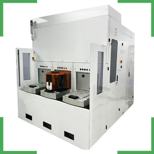
VERITY NEXTGEN
Compound Semiconductor | Advanced Packaging | HVM-High Volume Measurement
Compound Semiconductor Substrates, Glass, SiC
KEY FEATURES:
- Optimized for Compound Semiconductor Applications
- Advanced Packaging Compatibility
- Flexible Wafer Handling
- Supported wafer sizes: (150/200/300 mm)
PRODUCT LINEUP
CD-SEM | Critical Dimension
VeraSEM 3D
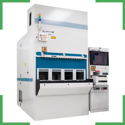
*Multiple Systems Available
NanoSEM 3D

*Defect Analysis System
VeritySEM®

*Defect Analysis System
VeritySEM®II
*Multiple Systems Available
VeritySEM®III

*Multiple Systems Available
VeritySEM®NextGEN
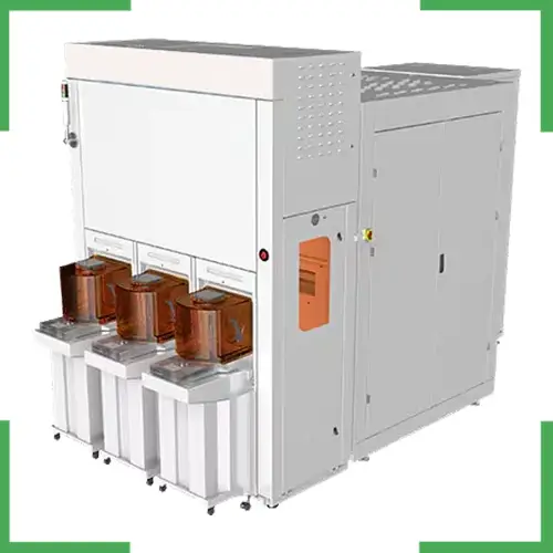
*Defect Analysis System
VeritySEM®4i (4i+)
*Defect Analysis System
VeritySEM®5i
*Multiple Systems Available
SUBMIT REQUEST FOR A QUOTE or INFO
QUICK LINKS
ETROLOGY
RTEX
METREX
EVENTS
CAREERS
CONTACT
EMAIL: sales@gt3i.com
PHONE: 480-400-6910
PHONE: 800-608-4834
LOCATION: 15936 N 78th St
Scottsdale, AZ 85260

Connect & Follow Us

